Versatile, cost-effective scanning electron microscope with integrated EDX for routine surface imaging and elemental analysis in industrial and academic environments.
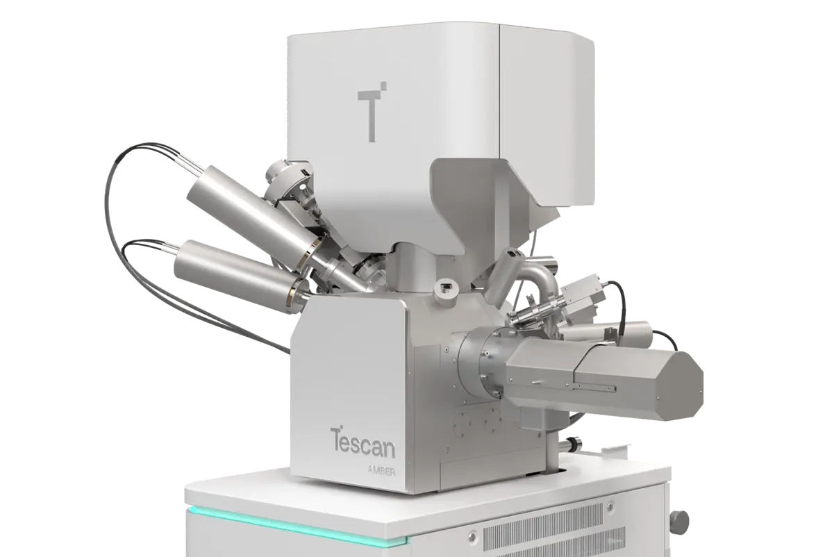
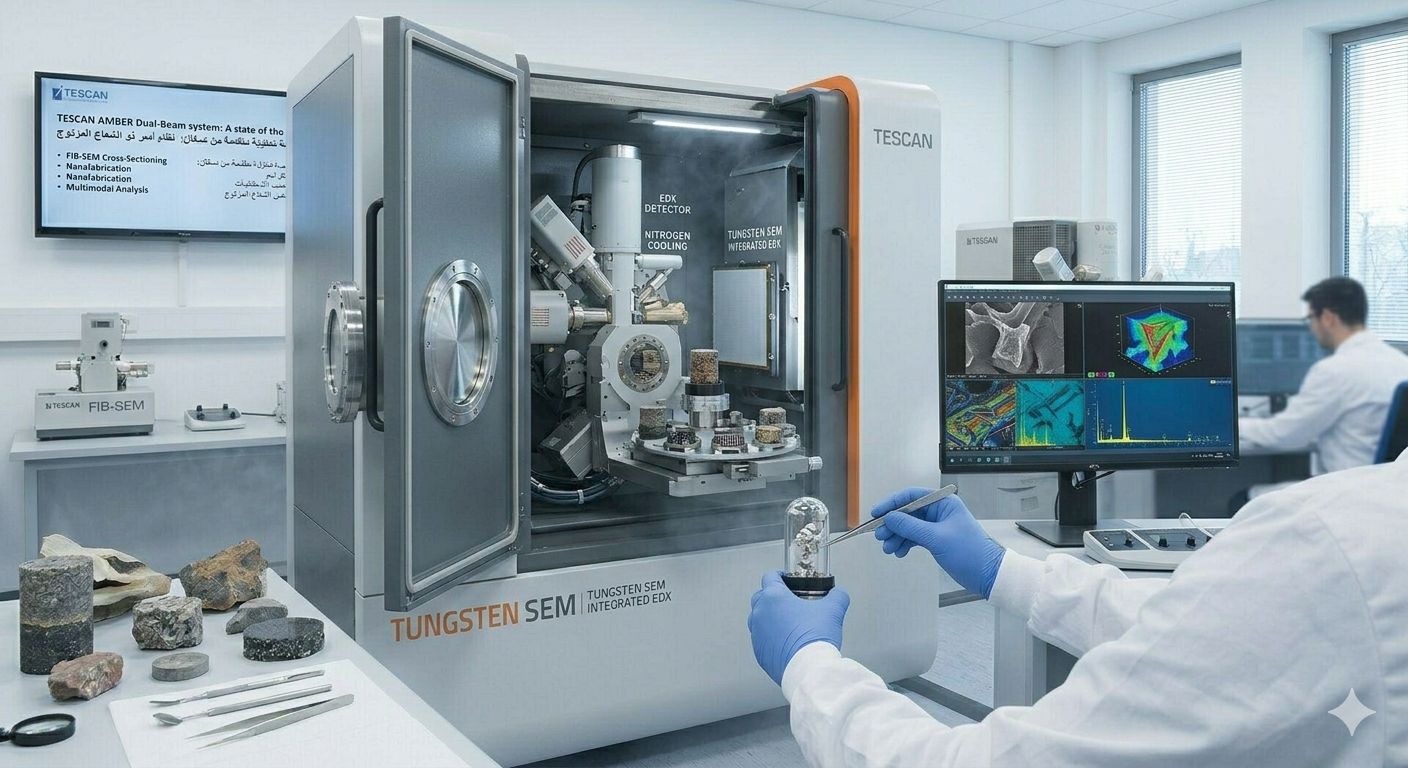
The TESCAN Tungsten SEM offers an excellent entry point into electron microscopy without compromising on image quality or analytical capability. Equipped with a robust thermionic tungsten gun and integrated EDX detector, it delivers reliable surface imaging and elemental mapping for a wide range of industrial and academic applications.
The TESCAN Tungsten SEM is designed to provide reliable, high-quality scanning electron microscopy at the most accessible price point in the TESCAN portfolio. Built around a robust thermionic tungsten gun, the instrument offers the imaging performance and analytical versatility needed for a broad range of routine and research applications.
Its standard Variable Pressure (VP) mode — operating at up to 2000 Pa — allows direct imaging of wet, oily, or non-conductive samples without any sputter coating preparation. This dramatically reduces turnaround time for industrial samples.
The integrated Silicon Drift Detector (SDD) for EDX enables fast, high-count-rate elemental analysis with excellent energy resolution. Full elemental mapping, line scanning, and point analysis are available directly within TESCAN ESSENCE™ software.
| SEM Resolution | 3.0 nm at 30 kV |
| Electron Source | Thermionic Tungsten Filament |
| Accelerating Voltage | 500 V – 30 kV |
| Magnification | 5× – 300,000× |
| Beam Current | 1 pA – 2 µA |
| Stage | 4-axis motorized (optional 5-axis) |
| Sample Size | Up to 100 mm diameter |
| EDX Detector | Silicon Drift Detector (SDD), > 125 eV resolution |
| EDX Elements | Be (4) to Pu (94) |
| Variable Pressure | Up to 2000 Pa (standard) |
| Detectors | SE, BSE, Robinson BSE |
| Software | TESCAN ESSENCE™ + EDX Analysis Suite |
Our scientific instrument specialists are ready to help you find the best solution for your research needs.