High-resolution field emission SEM delivering exceptional image quality and analytical performance for surface imaging, elemental analysis, and microstructure characterization.
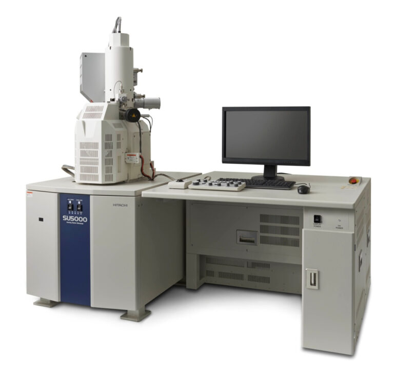
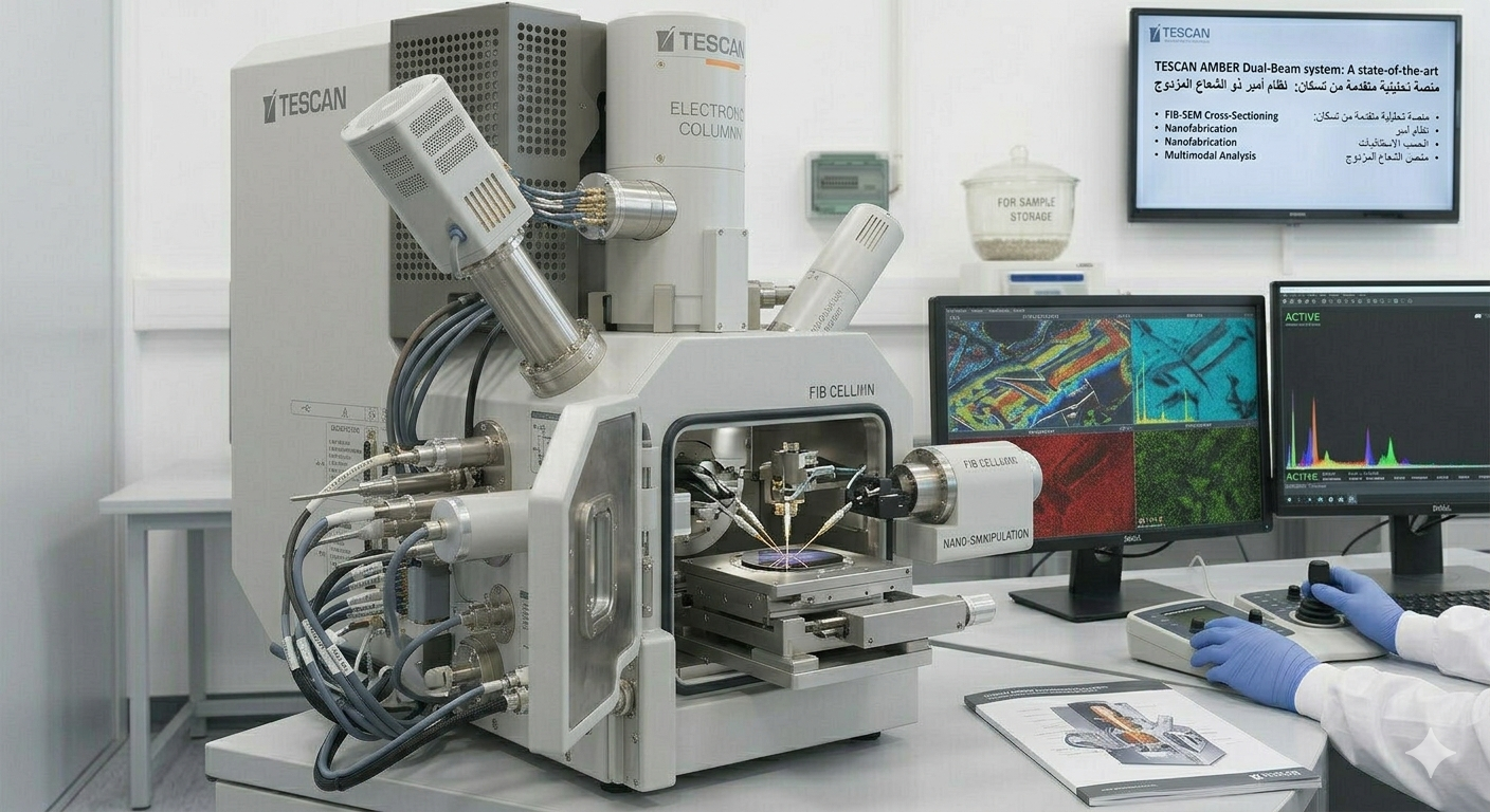
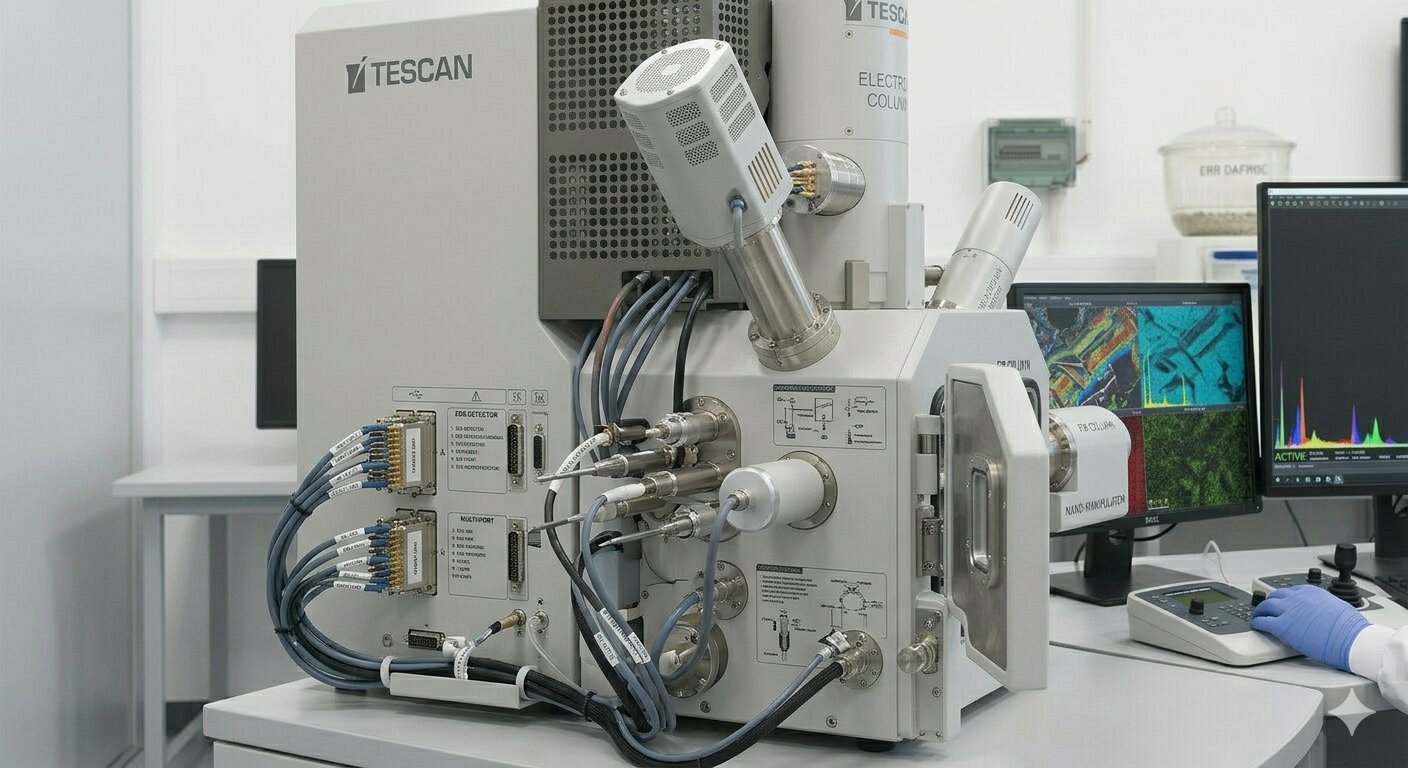
The TESCAN FE-SEM delivers outstanding high-resolution imaging and analytical capabilities for a wide range of materials. Its Schottky field emission gun provides exceptional brightness and beam coherence, enabling sub-nanometer resolution imaging alongside comprehensive elemental analysis using EDX, WDS, and EBSD detectors.
The TESCAN FE-SEM is a versatile high-resolution scanning electron microscope built around a Schottky thermal field emission gun (FEG). This electron source delivers superior brightness, low energy spread, and excellent spatial coherence — enabling crisp sub-nanometer imaging across a wide range of beam currents and accelerating voltages.
The instrument features TESCAN's innovative Wide-Field Optics (WFO) technology, which significantly extends the depth of field compared to conventional SEM designs. This is particularly valuable for imaging rough or complex sample surfaces without refocusing.
An optional Variable Pressure (VP) mode allows imaging of non-conductive samples without sputter coating, reducing sample preparation time and preserving surface integrity for sensitive specimens.
| SEM Resolution | 0.9 nm at 15 kV / 1.5 nm at 1 kV |
| Electron Source | Schottky Field Emission Gun (FEG) |
| Accelerating Voltage | 200 V – 30 kV |
| Beam Current | 1 pA – 400 nA |
| Magnification | 2× – 1,000,000× |
| Stage | 5-axis eucentric motorized |
| Sample Size | Up to 150 mm diameter |
| Detectors | SE, BSE, In-Beam SE/BSE |
| Optional Detectors | EDX, WDS, EBSD, CL, STEM |
| Vacuum | Oil-free, < 1×10⁻⁴ Pa |
| Software | TESCAN ESSENCE™ |
| Low Vacuum Mode | Up to 500 Pa (optional) |
Our scientific instrument specialists are ready to help you find the best solution for your research needs.